
Avoiding a Complete Redesign After a Panel Potentiometer was Made Obsolete
Challenge
The customer approached Vishay when their existing panel potentiometer supplier discontinued production of a part used on an established and popular piece of equipment. To avoid a costly redesign, an existing panel potentiometer needed to be adapted to meet the customer’s electrical requirements. It would also have to fit the control panel insertion / retention envelope and existing markings, in addition to the PCB assembly attachment system.

Solution
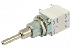
The Vishay P11 family consists of 12.5 mm single-turn panel potentiometers with numerous mechanical and electrical options, including resistance values between 20 Ω and 10 MΩ, integrated rotary and push-push switches, center tap and detent modules, and custom mechanical travel values between 90° and 300°.
The devices’ flexibility ensured that the customer’s previously used potentiometer could be replicated electrically. In addition, specifically matching the existing mechanical travel value eliminated the need for any changes in visual markings on the control panel cover itself, which saved a costly redesign and the associated wasted time.
Meeting the mechanical and manufacturing requirements would prove to be more complicated. The standard mechanical shaft options were not directly equivalent, and the knob didn’t match the others currently being used. In addition, the standard P11 through-hole pins used for soldering the potentiometer to the PCB would require a secondary manufacturing operation during assembly. A solderless PCB connection would therefore be a much more desirable and cost-effective solution.
Utilizing the P11 potentiometer body for this application meant it needed to be installed through a standard 22 mm diameter cut-out in the control panel, and, if possible, connected by a simple screw clamp like the other panel controls. To achieve this required integrating a custom shaft design that matched the panel’s existing knobs. These features were designed, and the custom shaft was integrated into the P11 body assembly, thereby enabling the existing knob to be added after insertion.
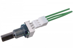
A solderless connection for fast and secure mounting on the panel was also desirable. Here the options included an IDC connector that was wire-attached to the potentiometer that could be easily pressed onto IDC pins already soldered into the PCB. This methodology avoided the need for a costly and time-consuming secondary hand-soldering operation.
Benefit
The customized P11 potentiometer that was designed and implemented for the customer was a perfect solution for their application. It avoided the need for a costly redesign and a secondary manufacturing operation that the standard connection pins would require. This significantly reduced the potential time that would be wasted, and the potential brand value lost by implementing a new look and feel on the control panel.
Additional Case Studies

Avoiding a Complete Redesign After a Panel Potentiometer was Made Obsolete
Challenge
The customer approached Vishay when their existing panel potentiometer supplier discontinued production of a part used on an established and popular piece of equipment. To avoid a costly redesign, an existing panel potentiometer needed to be adapted to meet the customer’s electrical requirements. It would also have to fit the control panel insertion / retention envelope and existing markings, in addition to the PCB assembly attachment system.


DC-Link Capacitors With Tab Terminals For Harsh Vibration Profiles
Challenge
Our customer was evaluating a solution for power electronics equipment that required the use of several DC-Link capacitors on the same PCB, while ensuring that the devices would support critical vibration profiles. The products being considered for the application had a significantly high mass of around 100 g, and were attached to the PCB via four lead wires with 1.2 mm diameters. While testing these parts under severe vibration profiles, the customer reported broken lead wires. The challenge was clear: how can such high mass parts withstand severe vibration profiles, while maintaining a similar footprint on the PCB?

mmWave Loss and Unstable Performance in a Satellite Payload
Challenge
While developing a next‑generation Ka‑band and W‑band satellite payload for a low‑Earth‑orbit communications constellation, an RF systems engineer encountered an unexpected challenge. Although the team designed a GaN power amplifier and low‑noise receiver chain to operate above 80 GHz, system testing revealed significant performance degradation. The active devices met their specifications, but once the signal left the die, system performance collapsed: Insertion loss exceeded the link budget by 1.5 dB Parasitic inductance from wire bonds and interconnects distorted matching Board-to-board variation caused gain and phase inconsistencies across flight units Commercial passive components were too large and introduced resonances above 70 GHz The design relied on an advanced organic PCB with thick‑film passives and LTCC modules. Despite extensive tuning and redesign cycles, performance drifted from build to build, introducing unacceptable risk to schedule and qualification.
Have questions? We can help.
This is our general contact form. If you have more specific questions or needs please select from the options below.